
ESP32-C6 Development Board
A breadboard-friendly ESP32-C6
with a 50 Ω RF path.
A development board built on the bare ESP32-C6 chip instead of a module, with battery charging, microSD and Qwiic on board. A 50 Ω RF path feeds a PCB antenna or u.FL, so it also serves as a reference for chip-down RF designs.
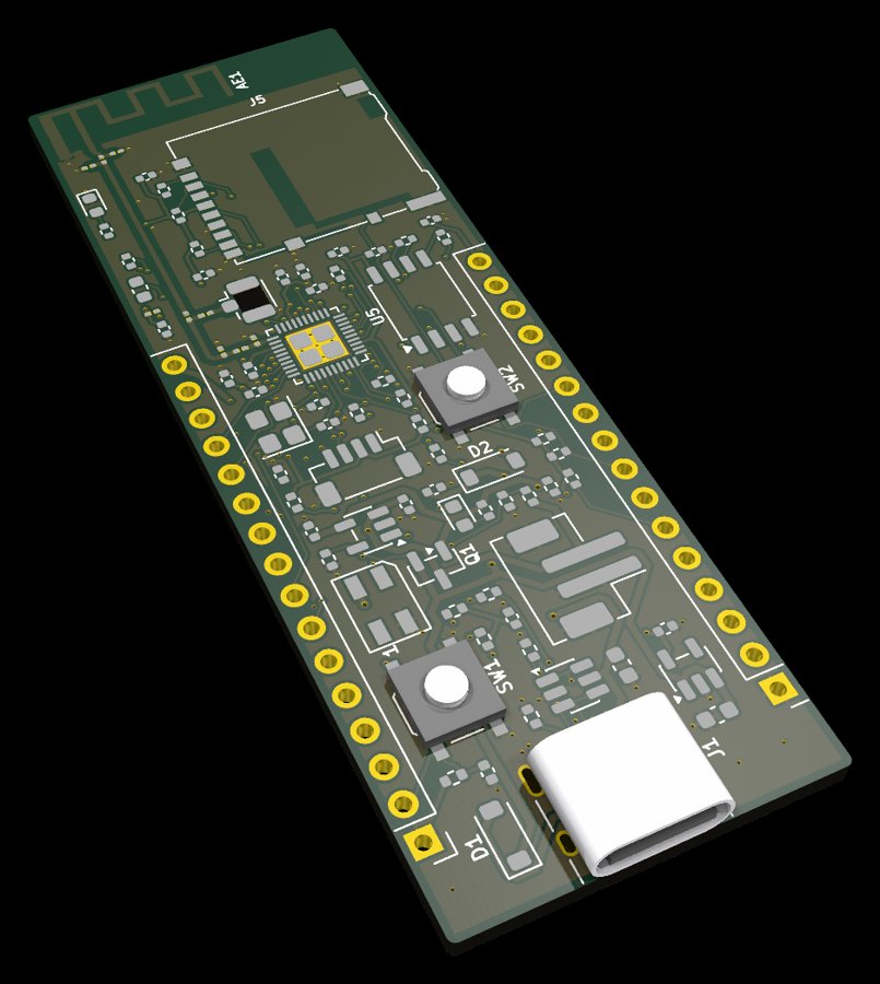
DESIGN RENDERING
Wi-Fi 6
2.4 GHz, on the ESP32-C6
BLE 5 + 802.15.4
Thread and Zigbee capable
25.4 × 72 mm
Four-layer board, parts on top
23 GPIO
All user pins on two 0.1 in headers
8 MB
W25Q64JV SPI flash
LiPo + USB-C
Charger with automatic switchover
RF
- TI AN043 PCB antenna or u.FL, chosen by a 0201 link
- 50 Ω microstrip RF feed
Power
- MCP73831 single-cell LiPo charger, JST-PH
- Battery voltage readable on GPIO0
- 3.3 V, 600 mA AP2112K LDO
USB
- USB-C for power and programming
- Built-in USB Serial/JTAG for flashing and console
- No separate USB-UART bridge
Peripherals
- Qwiic / STEMMA QT on the LP I²C pins
- microSD slot in SPI mode with card detect
- SK6812MINI RGB LED; BOOT and RESET buttons
Breadboard fit
- Two 1 × 16 0.1 in headers, 0.9 in apart
- Brings out 3V3, VSYS, VBAT, EN and GND
- Antenna and USB-C at opposite ends
Build
- Four-layer board, all parts on top
- Runs from USB-C or a single-cell LiPo
Building on the ESP32-C6?
Request a quote for boards or a custom chip-down design.
Request a Quote TodayFigures are design values or estimates, not measurements. Available for US Government use and as evaluation kits for product developers, software developers and system integrators. Export may be restricted under US export control regulations.